Using the STM32H5E5 SPI1 for continuous duplex comms
The aim has been to understand the timing relationship between the STM32H5E5 SPI1 transmit and receive FIFOs, particularly the internal transmit path between the TX FIFO and the serial output. This matters to the continuous SPI1 duplex comms developed in part for inclusion in Bill's Notes. The duplex comms receives constant data from cLog, transfers data to RAM in units of maximum FIFO capacity in this case comprising four 32-bit words, and needs to operate reliably for situations with reduced SYSCLOCK.
The engineering question is how much time the processor has to replenish the TX FIFO and service the RX FIFO while SPI communication continues without loss or error.
Device: STM32H5E5, SPI1 used as a slave
SPI mode: CPOL = 0, CPHA = 0
Frame size: 32 bits (DSIZE configured for 32-bit frames)
Transfer size: TSIZE = 0 (continuous transfer)
FIFO threshold: configured for four 32-bit frames (maximum FIFO capacity for SPI1)
PACKET: here packet is four 32-bit frames, equals maximum FIFO capacity for SPI1, equals 16 bytes
TX FIFO capacity: 16 bytes, equivalent to four 32-bit words
SCLK: 2 MHz
The duplex comms uses polling rather than any interrupts or DMA for the packet transfer. In our case TXP indicates that the TX FIFO is empty and has space for a new complete packet. RXP indicates that the RX FIFO is full and contains a complete packet. So we are operating in packets of complete FIFO content.
After loading the first packet the assembly code tests for TXP asserted and must preload a new packet into the TX FIFO. It then tests for RXP asserted and immediately reads a received packet into RAM. A packet is four 32-bit words written consecutively to SPI1_TXDR or read consecutively from SPI1_RXDR.
Tests found that at high SYSCLOCK, the measured interval between the TXP and RXP asserted was consistently 6.5 SCLK periods. TXP asserted very soon after a falling SCLK edge. RXP asserted very soon after a rising SCLK edge. The observed phase relationship was consistent with the CPOL = 0, CPHA = 0 SPI clocking. A 64 KB transfer completed without any reported UDR (transmit underrun) indication.
The absence of UDR and data integrity is strong evidence that the refill sequences work reliably, although it does not independently prove that every transmitted bit was correct over time.
The measurements indicate that, at this high SYSCLOCK, observed timing is dominated by SPI transfer progress rather than CPU execution speed.
The working hypothesis is that the internal TX shift register, or the effective transmit stage between the FIFO and serial output, operates at byte granularity and may be 8 bits wide.
The TX FIFO holds 16 bytes. The configured four-word packet also occupies 16 bytes. TXP indicates sufficient space for another complete packet. With this FIFO capacity, TXP assertion is associated with the TX FIFO becoming empty. Yet TXP must assert while transmission is still progressing, before the corresponding received packet is completely fills the RX FIFO and RXP asserts. The observed separation is approximately 6.5 SCLK periods. Accounting for the half-SCLK phase relationship of MISO gives an effective interval of approximately seven SCLK periods. This is much closer to a byte time than to a 32-bit word time. This supports suggesting an 8-bit transmit stage, but the physical width of the internal shift register has not been confirmed. The FIFO-to-shift-register transfer mechanism could produce similar external behaviour without a physically separate 8-bit shift register.
A useful conceptual model is to treat the TX FIFO as an egg timer. The FIFO contains a finite quantity of data, a packet, that is consumed as SCLK progresses. The FIFO capacity, configured data size and threshold describe the available storage and packet boundaries. The serial clock determines how quickly the stored data is consumed. This differs from the usual description of a FIFO as elasticity to accommodate irregular software service. In this continuous duplex comms, the FIFO is viewed as a known quantity of queued work that gives software a finite service interval. Therefore the time between service intervals is the maximum possible for the FIFO capacity and SCLK frequency.
The 32-bit frame size used is very convenient because the processor can perform 32-bit TXDR writes and RXDR reads. It does not establish that, or even need that the internal serial transmit path operates on 32-bit units.
The following assembler code example shows the mechanism at work. The example is structural rather than guaranteed working code. This continuous duplex comms completes the 64 KB transfer at quite low SYSCLOCK frequencies, potentially as low as 16MHz.
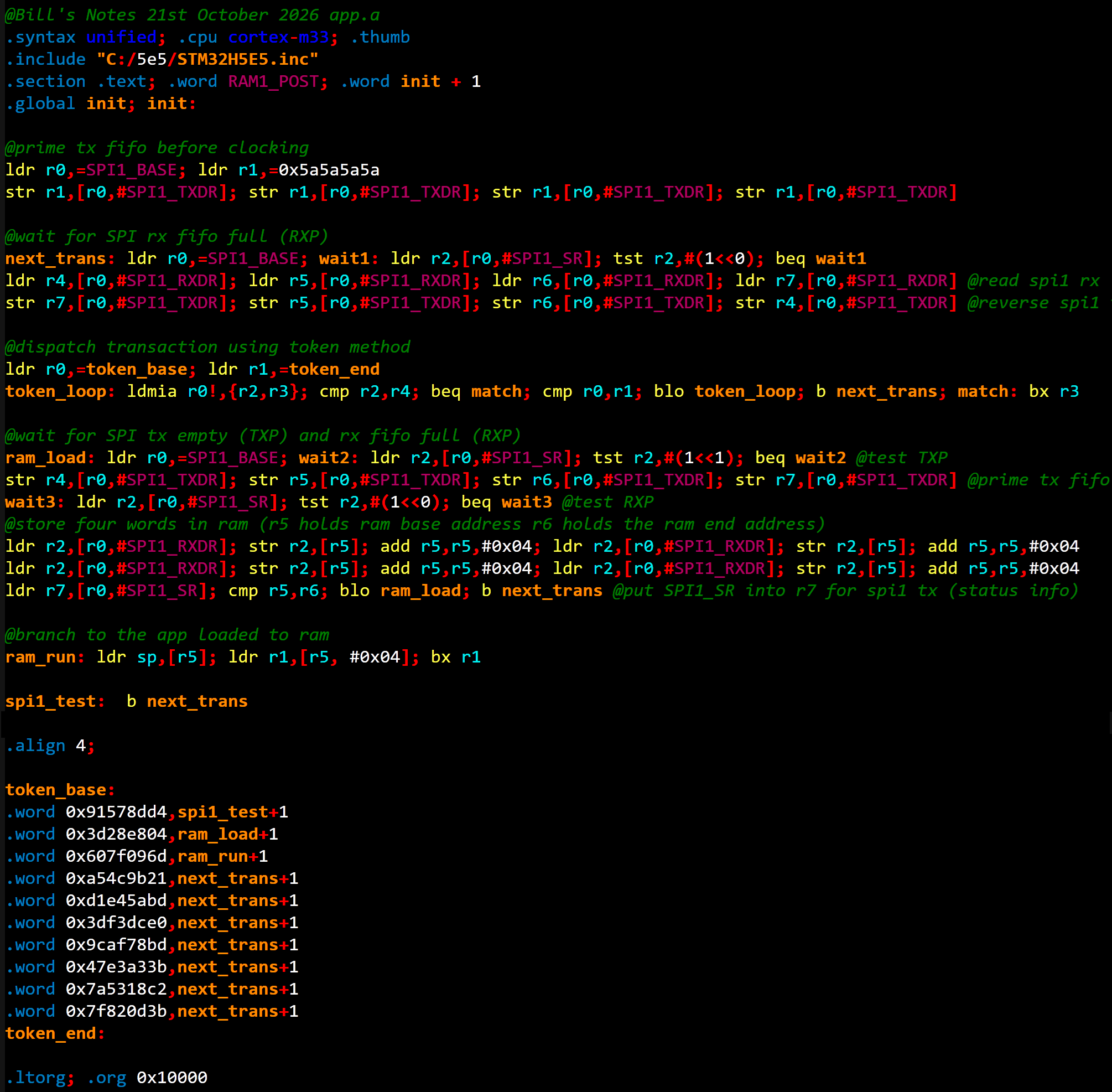
Briefly explaining the code. The TX FIFO is refilled immediately after TXP. The RX FIFO is drained immediately after RXP. FIFO capacity and serial clock establish a useful timing model for software service. The 64 KB test completes without any reported UDR indication at the higher, problems arise if the SYSCLOCK is below 16MHz. The practical success of the duplex comms does not depend on knowing the internal shift-register width. The value is in demonstrating a minimal, predictable and reusable continuous SPI duplex comms that really does run constantly without any time gaps. In other words SCLK runs constantly at 2 MHz for the entire 64KB transfer.
The length of block transferred was 64KB but it could be much longer. The limitation is that NSS is asserted during the entire transfer. Here are files used during code development.
The duplex comms source code app.a
The duplex comms linker file app.ld
The duplex comms include file STM32H5E5.inc